- 您现在的位置:买卖IC网 > Sheet目录1995 > DS4266P+ (Maxim Integrated Products)IC OSC CLOCK 266MHZ 10-LCCC
DS4266
DDR Clock Oscillator
_______________________________________________________________________________________
3
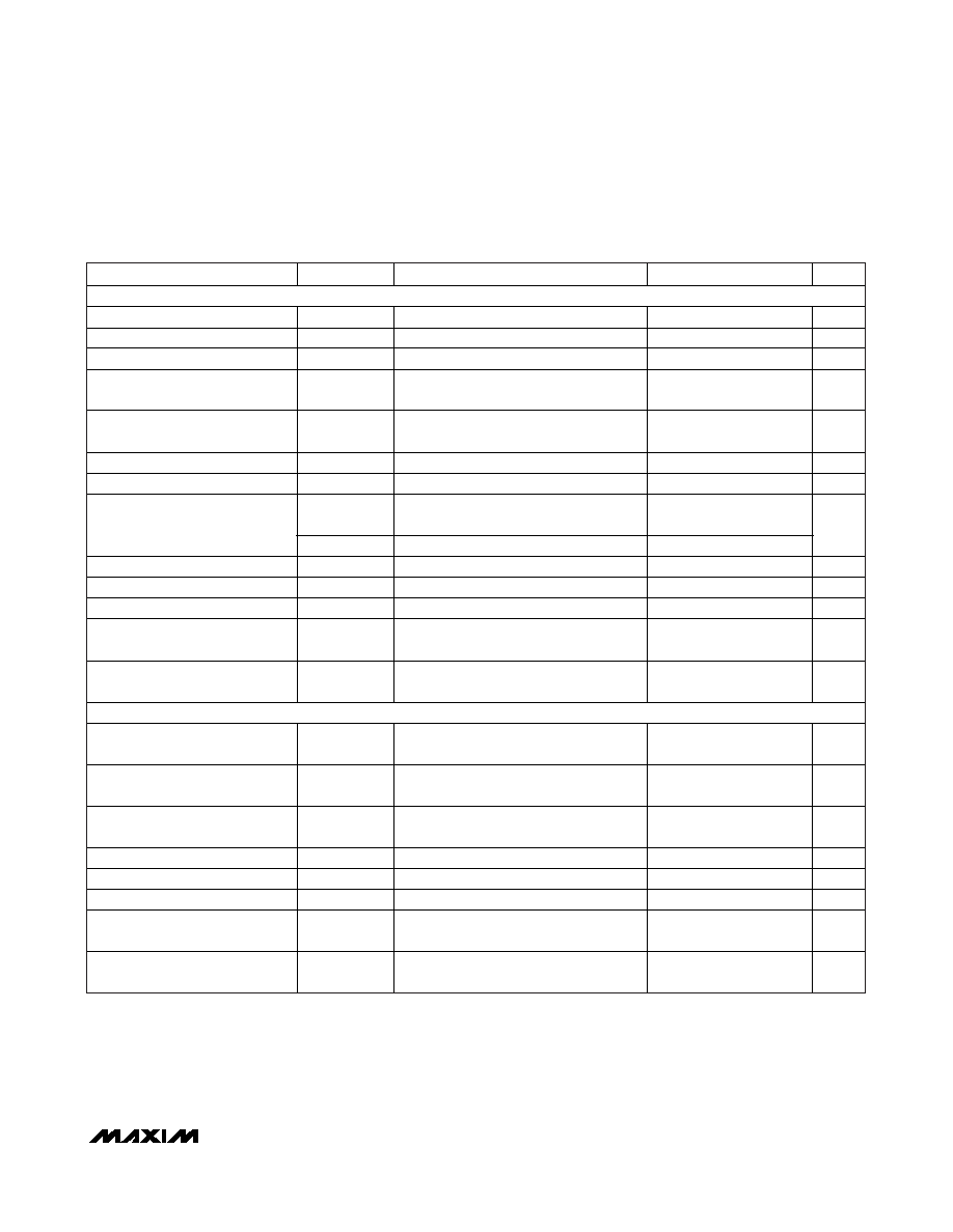
ELECTRICAL CHARACTERISTICS (continued)
(VCC = 3.135V to 3.465V, TA = -40°C to +85°C, unless otherwise noted.)
PARAMETER
SYMBOL
CONDITIONS
MIN
TYP
MAX
UNITS
LVDS
Output High Voltage
VOHLVDSO
100
differential load (Note 1)
1.475
V
Output Low Voltage
VOLLVDSO
100
differential load (Note 1)
0.925
V
Differential Output Voltage
|VODLVDSO|
100
differential load
250
425
mV
Output Common-Mode Voltage
Variation
VLVDSOCOM
100
differential load
150
mV
Change in Differential Magnitude
or Complementary Inputs
|VODLVDSO|
100
differential load
25
mV
Offset Output Voltage
VOFFLVDSO
100
differential load (Note 1)
1.125
1.275
V
Differential Output Impedance
ROLVDSO
80
140
LVSSLVDSO
OUTN or OUTP shorted to ground and
measure the current in the shorting path
40
Output Current
LLVDSO
OUTN or OUTP shorted together
6.5
mA
Output Rise Time (Differential)
tRLVDSO
20% to 80%
175
ps
Output Fall Time (Differential)
tFLVDSO
80% to 20%
175
ps
Duty Cycle
DCYCLE_LVDS
48
52
%
Propagation Delay from OE Going
Low to Logical 1 at OUTP
tPA1
200
ns
Propagation Delay from OE Going
High to Output Active
tP1A
200
ns
LVPECL
Output High Voltage
VOH
Output connected to 50
at PECL_BIAS
at VCC - 2.0V
VCC -
1.085
VCC -
0.88
V
Output Low Voltage
VOL
Output connected to 50
at PECL_BIAS
at VCC - 2.0V
VCC -
1.825
VCC -
1.62
V
Differential Voltage
VDIFF_PECL
Output connected to 50
at PECL_BIAS
at VCC - 2.0V
0.595
0.710
V
Rise Time
tR-PECL
200
ps
Fall Time
tF-PECL
200
ps
Duty Cycle
DCYCLE_PECL
48
52
%
Propagation Delay from OE Going
Low to Output High Impedance
tPAZ
200
ns
Propagation Delay from OE Going
High to Output Active
tPZA
200
ns
Note 1: All voltages referenced to ground.
Note 2: AC parameters are guaranteed by design and not production tested.
Note 3: Frequency stability is calculated as:
ΔfTOTAL = ΔfTEMP + ΔfVCC x (3.3 x 5%) + ΔfLOAD + ΔfAGING.
发布紧急采购,3分钟左右您将得到回复。
相关PDF资料
DS4302Z-020/T&R
IC DAC 5-BIT SGL 0-2.0V 8-SOIC
DS4302Z-020+
IC DAC 5-BIT SGL 0-2.0V 8-SOIC
DS4311P+
IC OSC CLOCK 311.04MHZ 10-LCCC
DS4404N+
IC DAC 4CH I2C ADJ 14-TDFN
DS4412U+
IC DAC DUAL CH I2C ADJ 8-USOP
DS4424N+
IC DAC 7BIT 4CH 5.5V 14-TDFN
DS4425BN+
IC OSC CLOCK 425MHZ 10-LCCC
DS4426T+T&R
IC DAC I2C-MARGINING 4CH 28-TQFN
相关代理商/技术参数
DS428
制造商:未知厂家 制造商全称:未知厂家 功能描述:Analog IC
DS42-AV
制造商:TATUNG 功能描述:COMMERCIAL GRADE LCD MONITOR, HORIZONTAL OR VERTICAL VIEWING, NATIVE RESOLUTION
DS42BR400
制造商:NSC 制造商全称:National Semiconductor 功能描述:Quad 4.25 Gbps CML Transceiver with Transmit De-Emphasis and Receive Equalization
DS42BR400_07
制造商:NSC 制造商全称:National Semiconductor 功能描述:Quad 4.25 Gbps CML Transceiver with Transmit De-Emphasis and Receive Equalization
DS42BR400_08
制造商:NSC 制造商全称:National Semiconductor 功能描述:Quad 4.25 Gbps CML Transceiver with Transmit De-Emphasis and Receive Equalization
DS42BR400-EVK
功能描述:其他开发工具 DS42BR400 EVAL BOARD
RoHS:否 制造商:Parallax 产品:ELEV-8 Hex Upgrade Kits 类型:Robotics 工具用于评估:ELEV-8 Quadcopter 工作电源电压:
DS42BR400TSQ
功能描述:总线收发器 RoHS:否 制造商:Fairchild Semiconductor 逻辑类型:CMOS 逻辑系列:74VCX 每芯片的通道数量:16 输入电平:CMOS 输出电平:CMOS 输出类型:3-State 高电平输出电流:- 24 mA 低电平输出电流:24 mA 传播延迟时间:6.2 ns 电源电压-最大:2.7 V, 3.6 V 电源电压-最小:1.65 V, 2.3 V 最大工作温度:+ 85 C 封装 / 箱体:TSSOP-48 封装:Reel
DS42BR400TSQ/NOPB
功能描述:总线收发器 RoHS:否 制造商:Fairchild Semiconductor 逻辑类型:CMOS 逻辑系列:74VCX 每芯片的通道数量:16 输入电平:CMOS 输出电平:CMOS 输出类型:3-State 高电平输出电流:- 24 mA 低电平输出电流:24 mA 传播延迟时间:6.2 ns 电源电压-最大:2.7 V, 3.6 V 电源电压-最小:1.65 V, 2.3 V 最大工作温度:+ 85 C 封装 / 箱体:TSSOP-48 封装:Reel